8. 可编程逻辑[英]
本文最后更新于 2025年9月1日 上午
Programmable Logic
A dedicated logic circuit will only perform the function it was designed to implement.
A combinational circuit behaves according to its truth table, whereas a sequential circuit’s characteristics are governed by its state table.
In a programmable logic system, a standard hardware structure is electronically reconfigurable so that the different logic operations can be performed, without having to change the circuit physically.
Multiplexer
The multiplexer (多路复用器) is a multi-input, single-output circuit whose prime function is to convert parallel data to serial data.
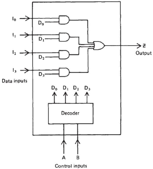
One multiplexer has two input end: the data input and control input.
The data input is used to give the data to each channel. Control input is used to determine which channel will be the output. The control input is realized by a decoder.
For example: a 4 to 1 Multiplexer uses two input variables to select which channel will be outputed: \(D_0=\overline{A}.\overline{B}\), \(D_1=\overline{A}.B\), \(D_2=A.\overline{B}\), \(D_3=A.B\).
For example, if \(AB=10\), then \(D_2\) is open.
It can be identified that, the variable used to be as control signal must contains all the possiblities: (from 00..0 to 11..1).
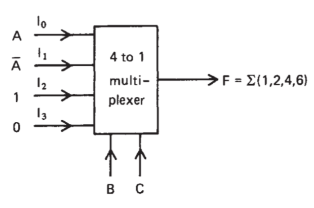
Multiplexer Used as Combinational Logic Design
For multiplexers, they can be used to design a combinational logic.
For a \(N\)-variable combinational logic function with \(M\) to 1 multi-plexer, the \([log_2M]\) variables will be used as control inputs, the other \(N-[log_2M]\) variables will be used as data input.
For 1st canonical form, the combinational logic function can be transfered into:
\[F=F_1C+F_2\overline{C}\] where \(F_1\) and \(F_2\) are data inputs, \(C\) is the control input.
Example: \(F(ABC)=∑(1,2,4,6)\):
\[F(A,B,C)=\overline{A}\overline{B}C+AB\overline{C}+A\overline{B}\overline{C}+AB\overline{C}\]
If 4 to 1 multi-plexer are used, then \(log_24=2\) control variables will be used. Here, suppose \(B,C\) are control varibles, then:
\[\begin{aligned}
F(A,B,C)&=\overline{B}\overline{C}(F_1)+\overline{B}C(F_2)+B\overline{C}(F_3)+BC(F_4)\\
&=\overline{B}\overline{C}(A)+\overline{B}C(\overline{A})+B\overline{C}(1)+BC(0)
\end{aligned}\]
Thus, the implementation diagrams are:
The rules of extracting control variables are:
- all terms (from all 0s to all 1s) should be satified.
- if there is not a certain control varible in a term, then the term should be rewriten as: \(F_1(C+\overline{C})\).
For example: \(ABD\),\(C\) is control varible, then this term should be rewriten as \(ABD(C+\overline{C})\).
- if there is not a certain data varible in a, then this term should be rewriten as: \(C.(1)\) or \(\overline{C}.(1)\).
Multilayer Multiplexer System
In multilayer multiplexer system, there are more than one floor of multiplexers.
The logic functions of \(n-1\) layer is generated by the \((n-1)\) th layer.
The size of the multiplexers and the number of layers will depend on the complexity of the function to be performed.
Example: \(𝐹 = ∑(1,2,4,5,7,8,12,17,19,21,28)\)
In this function, 5 variables will be used.
\(F(V, W, X, Y, Z)=00001+00010+00100+00101+00111+01000+01100+10001+10011+10101+11100\)
Condense \(F\) with \(YZ\):
\[\begin{aligned}
&F=(F_1)\overline{YZ}+F_2\overline{Y}Z+F_3Y\overline{Z}+(F_4)YZ\\
&F_1=(\overline{VW}X+\overline{V}W\overline{X}+\overline{V}WX+VWX)\\
&F_2=(\overline{VWX}+\overline{VW}X+V\overline{WX}+V\overline{W}X)\\
&F_3=(\overline{VWX})\\
&F_4=\overline{VW}X+V\overline{WX}
\end{aligned}\]
Then exapanding \(F_1,F_2,F_3\) and \(F_4\) about \(WX\) gives:
\[\begin{aligned}
&F1=(0)\overline{WX}+(\overline{V})\overline{W}X+(\overline{V})W\overline{X}+(1)WX\\
&F2=(1)\overline{WX}+(1)\overline{W}X+(0)W\overline{X}+(0)WX\\
&F3=(\overline{V})\overline{WX}+(0)\overline{W}X+(0)W\overline{X}+(0)WX\\
&F4==(\overline{V})\overline{WX}+(V)\overline{W}X+(0)W\overline{X}+(0)WX
\end{aligned}\]
Thus, the 2-layer diagram is:
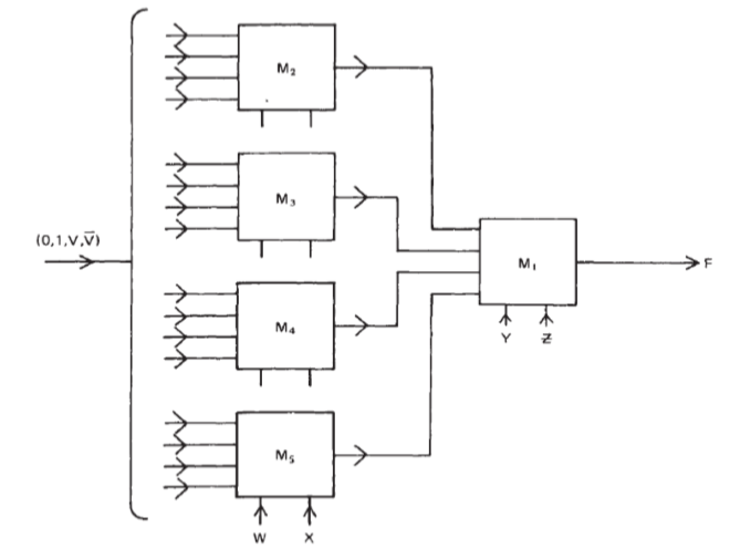
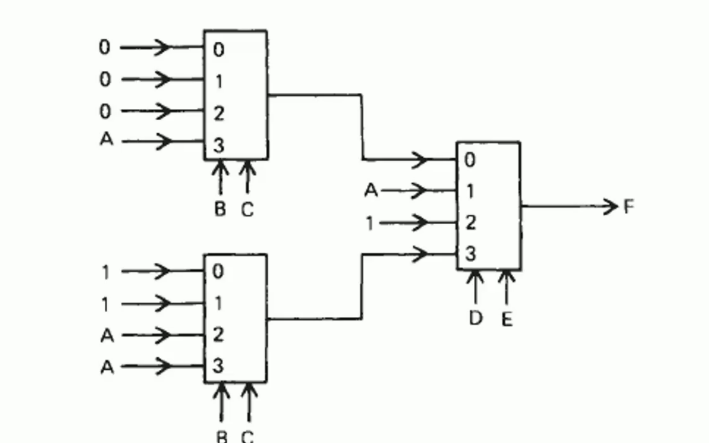
Example: 2 two-layer system of 4 to 1 multiplexers
\[F=ABC+\overline{AB}D+D\overline{E}+AE\] There are 5 variables, for one layer, 2 variables will be used as control bits, for the other layer, another 2 bits will be used as control bits.
For the 1st layer, DE will be chosen as control bits.
\[F=(F_0)\overline{DE}+(F_1)\overline{D}E+(F_2)D\overline{E}+(F_3)DE\] Just adding terms of \(DE\):
\[F=ABC(\overline{DE}+\overline{D}E+D\overline{E}+DE)+\overline{AB}D(\overline{E}+E)+AE(\overline{D}+D)\] \[\begin{aligned}
&F_0=ABC=(0)\overline{B}C+(0)B\overline{C}+(A)BC+(0)\overline{BC}\\
&F_1=ABC+A=ABC+A(BC+\overline{BC})=(A)BC+(A)\overline{BC}+(0)B\overline{C}+(0)\overline{B}C=A(BC+\overline{BC})=A\\
&F2=1\\
&F3=ABC+\overline{AB}+A=A(BC+B\overline{C}+\overline{B}C+\overline{BC})+\overline{AB}(C+\overline{C})=(A)BC+(1)\overline{BC}+(1)\overline{B}C+(A)B\overline{C}\\
\end{aligned}\]
The circuit diagram is:
Memory
A memory circuit contains several storage elements that can be addressed by a decoder circuit.
(Here decoder can be regarded as a multiplexer circuit.)
In this kind of circuit, the data will be first inputted into every functional parts of the system, then address will decide which part will be functional.
The data is introduced into the functionable part of system, this procedure is called read(读取).
The data from the functionable part is outputted to the final function, this procedure is called write(写入).
Read and write are controlled by clock pulse.
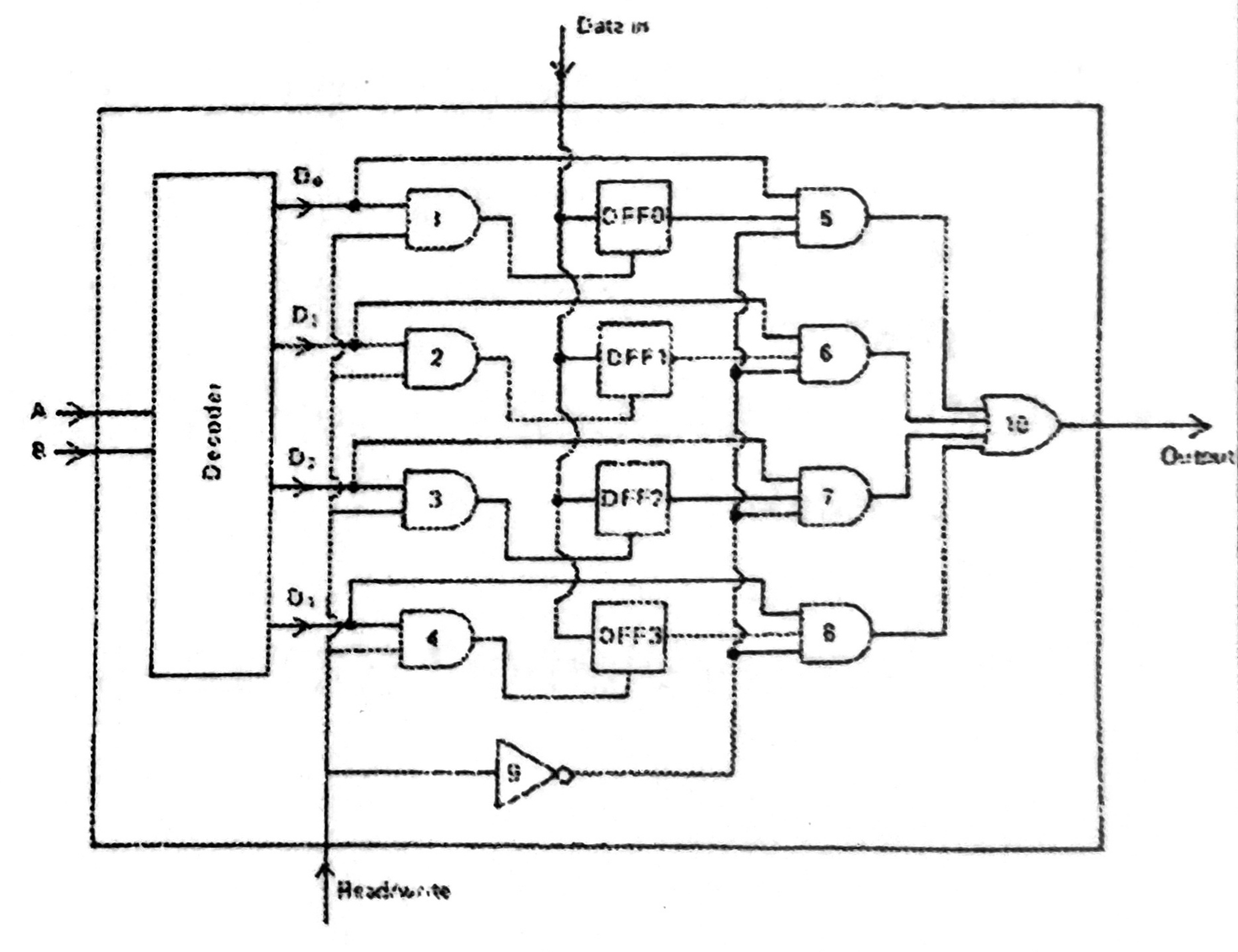
For example, above circuit is a 4-bit random access memeory. \(AB\) is used as a control varible to determine which channel will be outputted.
The R/D control line controls the read and write of memeory.
When \(R/D=0\), the decoder cannot output one channel due to the input of AND gates are 0s. And all DFF’s \(clk=0\), data can be writen into DFFs and held for a clock pulse, that is a write mode of memeory.
When \(R/D=1\), the decoder output one channel. And all DFF’s \(clk=1\), DFF will output the result to the end, that is a read mode of memeory.
Address(地址)
The code inputted into the decoder to control which part will be functioned is named as address. Address corresponds to a functionality or corresponds to one bit input.
The storage of memory is \(2^n\), \(n\) is the number of addresses bits(input addresses and function addresses).
Random Access Memory (RAM)(随机寄存器/缓存)
The memory locations may be read and written to any Output sequence without having to be scanned.
It’s called Random.
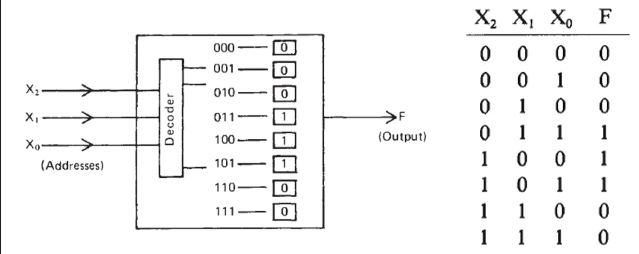
Combinational Logic Using Memory
A memory can act as a logic function simply by storing a truth table, and as any truth table can be loaded into store, the device is both programmable and universal. A memory is programmed to perform a combinational logic function by first obtaining the complete truth table of the function.
Example: Design a combinational logic system based on a memory, which will indicate when a 3-bit binary number \(X\) is in the range \(3≤X≤5\).
Byte Organized Memories
Byte-organized memories can be set to implement multi-output functions.
The address field can be partitioned into two parts, to enable more than one function to be programmed into a large memory.
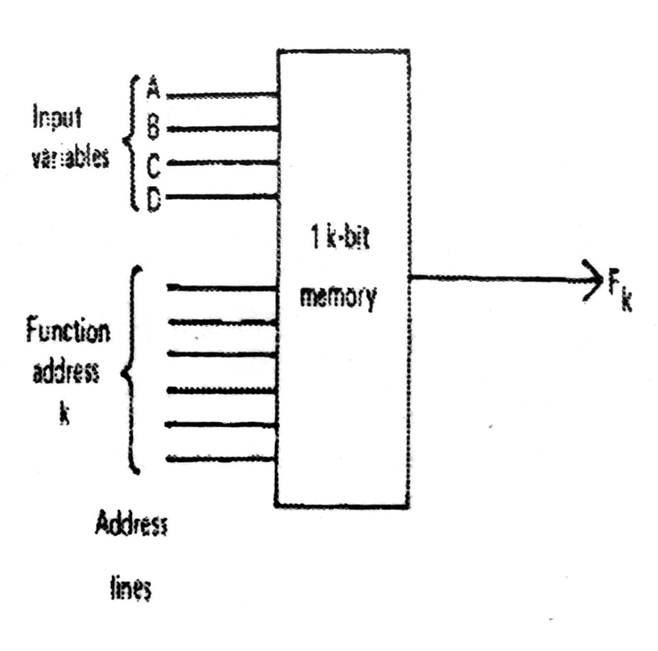
For example, for a 1k (\(2^{10}\)) bit memory, there are 10 input lines. Four input lines will be used to input the data. The other 6 lines used to access the logic functions.
It can store \(2^6\) logic functions.
Sequential Logic using Memory elements
A memory circuit can be programmed to perform a sequential logic function provided feedback is incorporated into the system.
The address field is partitioned into the external data inputs and the internal states which are fed back from the output.
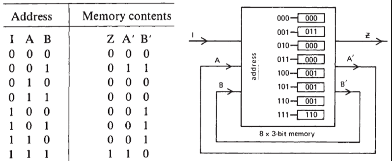
Example: 101 sequence detector
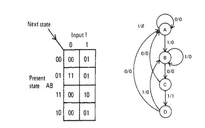
The address to memory must comprise
- a 3-bit address field
- The present state (2 bits)
- The external state (1 bit)
- The present state (2 bits)
- the output from the memory provides
- The logic system’s output Z (1 bit)
- The next states A’ and B’(2 bits)
- The logic system’s output Z (1 bit)
The memory needs to be organized in 3-bit bytes giving a minimum requirement of 8 x 3 bits.
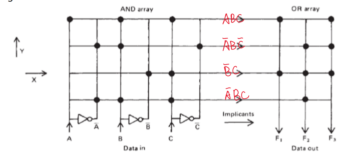
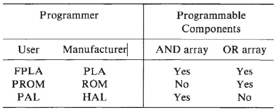
Programmable Logic Arrays and Programmable Arrays of Logic
Programmable Logic Arrays
A programmable logic array (PLA) can be regarded as a memory circuit with a programmable decoder. The matrix is divided into 2 parts
- the AND Array (equivalent to the decoder)
- the OR Array (the store)
Data is input via the \(Y\) wires into the AND array The horizontal \(X\) wires in the AND array perform the AND function.
The connections to the vertical \(Y\) wires in the OR array perform the OR function.
Example:
Below shows the PLA of three logical functions:
\[F_1=ABC+\overline{B}C\]
\[F_2=\overline{A}B\overline{C}+\overline{B}C+\overline{A}BC\] \[F_3=ABC+\overline{B}C+\overline{A}B\overline{C}\]
Conversion to PLA form
A logic system must be minimized so that its set of implicants can be accommodated within the PLA.
The system has be sufficiently minimal, so Kmap will be used.
The total number of implicants(Functions) does not exceed the number of \(X\) lines.
Programmable Arrays of Logic(PALs)
A PAL has a programmable AND array but a fixed OR array, where each output is a function of a pre-wired number of product terms
- The AND array is not universal
- The number of product terms that can be set up for an n input PAL is considerably less than \(2^𝑛\).
Example: 3-bit Gray code converter
For input \(CBA\):
\[X=A\]
\[Y=\overline{A}B+A\overline{B}=A XOR B\]
\[Z=\overline{B}C+B\overline{C}=B XOR C\] The PAL must generate \(Y\) and \(Z\) (no logic is required for \(X\)).
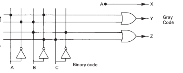
PALs can be programmed either by the user or during the last stage of manufacture using a metallic layer to form the desired connections.
Hard Arrays of Logic
Non-volatile devices are sometimes called hard arrays of logic or HALs.
The relationship between HALs and PALs is the same as that between ROMs and PROMs.
HALs are factory programmable and suitable for mass production.
Microprocessor
The microprocessor itself can now be regarded as a component in a digital system.
It is extremely flexible and can be programmed to perform complex logical and arithmetical operations.
A microprocessor can therefore only be regarded as a viable component of a larger digital system if the desired operations and response times are relatively slow.